
Can a circuit’s design width be comparable with a virus?
| Reference | Dimension |
|---|---|
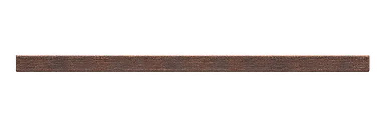
| SKY130 polysilicon line | 150 nm minimum design width: 150 nm |
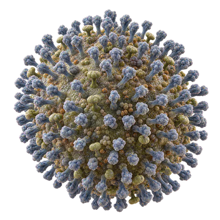
| Influenza virus | 100 nm Representative diameter |
Calculation: 150 nm ÷ 100 nm, after conversion into the same unit. The ratio calculated from the catalogue data is about 1.5.
Both illustrations use a common factor for the stated dimension. Positions aid reading and do not represent physical separation.
A design rule is not a measurement of every fabricated pattern and does not describe the whole transistor. Viruses vary between particles. The line segment’s length is cropped and symbolic; only its vertical width is to scale.
Check the conventions
SKY130 polysilicon line
PDK 2020Publication of the open PDK
The open SKY130 PDK gives 0.150 µm for the poly.1a rule, “Width of poly”. Polysilicon is used, among other things, to define transistor gates. This value is a minimum circuit layout rule, not a measurement of every line after fabrication; particular devices use other limits. Here, only the strip's vertical width is compared; its length is symbolic. The process name “130 nm” is a different concept.
Official Google/SkyWater PDK consulted on 28 October 2026, docs/rules/periphery-rules.rst, rule poly.1a “Width of poly”: 0.150 µm. Nominal design value; no physical measurement of the illustration.
Influenza virus
Viral particles have varied shapes and diameters. Displayed dimension: representative diameter.
Catalogue value to check against the source; not individually audited.
Choose another reference
Replace an object in the explorer, keep the common scale factor and try predicting the new ratio before reading it.
Open the comparison →