
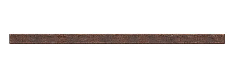
What does this number measure?
The open SKY130 PDK gives 0.150 µm for the poly.1a rule, “Width of poly”. Polysilicon is used, among other things, to define transistor gates. This value is a minimum circuit layout rule, not a measurement of every line after fabrication; particular devices use other limits. Here, only the strip's vertical width is compared; its length is symbolic. The process name “130 nm” is a different concept.
Compare the stated dimensions
The comparison uses the number in each fact sheet: altitude, height, diameter, length or distance, depending on the reference. Two values in metres do not necessarily describe the same property.
Source and limitations
Official Google/SkyWater PDK consulted on 28 October 2026, docs/rules/periphery-rules.rst, rule poly.1a “Width of poly”: 0.150 µm. Nominal design value; no physical measurement of the illustration.
Only the vertical width of the polysilicon line is compared; its horizontal length is symbolic. A layout rule, not metrology from a photograph.
Publication of the open PDK: PDK 2020. Official Google/SkyWater README actually consulted on 28 October 2026: the text places the project in May 2020 (“As of May 2020”) and describes an earlier mature process. Annual reference for publication of the open PDK, without claiming to date the first fabrication of a 150 nm line. The process and its widths existed before the PDK was made openly available. This does not mean that the 150 nm line was invented in 2020.