
What does this number measure?
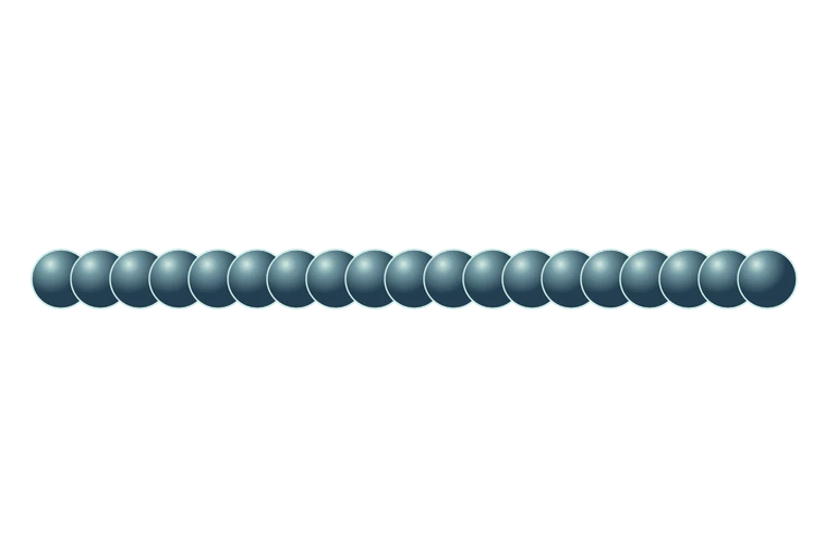
In 2022, the team of Fan Wu, He Tian and Tian-Ling Ren published a vertical MoS₂ transistor whose gate uses the edge of a graphene layer. The reported physical gate length is 0.34 nm, or 340 picometres. Only this dimension is compared, not the dimensions of the entire transistor, its contacts or a chip. The drawing isolates the gate's cross-section; its horizontal extent is symbolic. The effective channel length depends on the electrical state and must not be confused with this physical dimension. This laboratory result is among the shortest gates published; it is neither a commercial component nor permanent certification of a world record.
Compare the stated dimensions
The comparison uses the number in each fact sheet: altitude, height, diameter, length or distance, depending on the reference. Two values in metres do not necessarily describe the same property.
Compare with Experimental transistor · 1 nm nanotube gate in the explorer →
Source and limitations
Reference: Nature 603, 259–264 (2022), DOI 10.1038/s41586-021-04323-3. Abstract consulted in PubMed PMID35264756, with the 0.34 nm dimension in the indexed figure caption and the IEEE Spectrum summary. No measurement of the illustration; no total device size inferred.
Graphene gate cross-section: only the vertical thickness represents the physical gate length of 0.34 nm. The width, atomic spheres and bonds are symbolic; the complete transistor is not depicted. Non-photographic diagram.
Experimental publication: 2022. PubMed consulted: online publication on 9 March 2022. Publication date, not the manufacturing date of the illustrated device.