
One question, several references
How we learned to build things so small
From early microprocessors to complete 50-micrometre chips, then nanometre-scale details: understand what humans can manufacture without confusing packages, silicon and transistors.
Try it in the explorer →1971: bringing together about 2,300 transistors
A transistor can act as a tiny electronic switch in a digital circuit. Introduced in 1971, the Intel 4004 brings together about 2,300 transistors on a few millimetres of silicon. Its longer side is taken here as about 4 mm. This count is a historical reference; it measures neither speed nor operations per second.
1978: more functions, not necessarily a smaller chip
The 1978 Intel 8086 brings together about 29,000 transistors with a different architecture. Its silicon is taken here as about 6 × 5.5 mm. Progress therefore does not simply mean shrinking the entire object: more functions and transistors can also be combined over a larger area. Both historical counts are documented orders of magnitude, not values rechecked online in this session.
Package and silicon: two things to keep separate
The package protects the chip and connects it to the outside. Our 4004 package reference is about 20 mm long, compared with about 4 mm for the longer side of the silicon: a length ratio of 5. The Core i9-14900K’s 45 mm also describes a package, not the size of a transistor. Comparing these 45 mm with the 4004’s 4 mm of silicon does not measure processor miniaturisation or computing power.
Yes, complete chips can be much smaller
The Hitachi µ-chip reference is a version with a side length of 0.4 mm; other versions exist, so the chosen version matters. The Hitachi RFID demonstrator introduced in 2007 has a side length of only about 50 micrometres: a whole silicon chip, but with an external antenna and reader. Compared with the 8086’s 6 mm, that gives a length ratio of 120. It is not a computer with the same functions reduced 120 times.
What about a 0.3 mm device?
The experimental Michigan device presented in 2018 is taken as about 0.3 mm per side. It uses external optical infrastructure; it is not a self-contained PC. Miniaturising an identification tag, a specialised sensor or a general-purpose processor involves different problems. To understand a very-small-chip announcement, always ask what function it performs and what remains outside.
A wire thinner than a hair
A bonding wire can connect a chip’s contacts to its package. Our gold wire has a representative diameter of 25 micrometres. The example hair has a diameter of 70 micrometres, about 2.8 times greater. These are two diameters: the long drawn segments are there only to make the objects recognisable.
A width comparable with a virus
The open SKY130 PDK gives a minimum design rule of 150 nanometres for a polysilicon line. This is about 1.5 times the 100-nanometre diameter adopted for an influenza virus. The comparison helps visualise the designed detail; it does not turn a design rule into a measurement of every fabricated line or the size of an entire transistor.
Descending towards the nanometre
In a 2016 Berkeley demonstrator, a nanotube about 1 nanometre in diameter serves as the gate. DNA has a diameter of about 2 nanometres. It is the gate being compared, not the entire transistor with its contacts. Even a 50-micrometre chip still has a side length of 50,000 nanometres: a complete chip and a nanometre-scale detail are two different scales.
What this evolution tells us
We have learned to design, manufacture, connect and operate structures at several scales. Distinguish the number of integrated functions, component density, a detail’s dimensions and the complete system’s size. A commercial generation name such as “3 nm” is not a universal dimension of all transistors. The images interpret these objects and do not replace a metrology view.
Five comparisons to see the differences
Core i9 and Intel 4004: package versus silicon die
Can we compare the Core i9’s 45 mm with the Intel 4004’s 4 mm?
Intel 8086 and a 50-micrometre RFID chip: a length ratio of 120
How can a complete chip be 120 times shorter than an Intel 8086?
Bonding wire and hair: comparing two diameters
Is a chip’s bonding wire thinner than a hair?
Silicon line and virus: what does 150 nanometres mean?
Can a circuit’s design width be comparable with a virus?
Transistor gate and DNA: two diameters of a few nanometres
What does the nanometre in a laboratory transistor actually measure?
This journey’s references
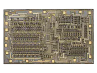 Microelectronics · 1971Intel 4004 · bare die4 mm
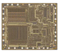 Microelectronics · 1978Intel 8086 · bare die6 mm
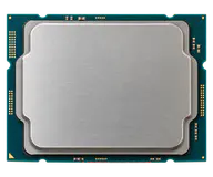 Microelectronics · 2023Core i9-14900K · package4.5 cm
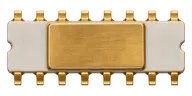 Microelectronics · 1971Intel 4004 · DIP package2 cm
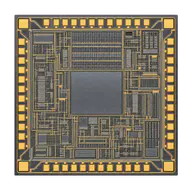 Microelectronics · Early 2000sHitachi µ-chip · 0.4 mm400 µm
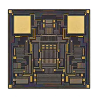 Microelectronics · 2007Hitachi · 50 µm RFID chip50 µm
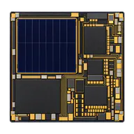 Microelectronics · 2018Michigan · 0.3 mm microdevice300 µm
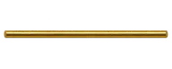 Microelectronics · Varies by periodGold bond wire25 µm
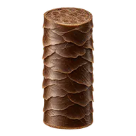 MicrocosmHuman hair70 µm
 Microelectronics · PDK 2020SKY130 polysilicon line150 nm
 MicrocosmInfluenza virus100 nm
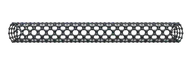 Microelectronics · 2016Experimental transistor · 1 nm nanotube gate1 nm
 MicrocosmDNA2 nm
Sources and method
Dimensions and conventions are those of the fact sheets linked above. Illustrations remain interpretations. Providing a documentary source does not independently certify every catalogue value.